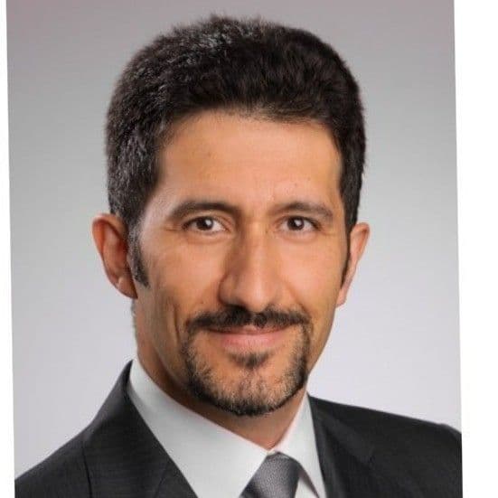
Bahram Nejand
Group Manager Memory Technology @ Fraunhofer Institute for Photonic Microsystems IPMS
About
As an accomplished Technology Manager with over a decade of experience, I have a proven record of driving innovation, leading cross-functional teams, and delivering technology-to-product transitions across advanced materials and semiconductor industries. Currently serving as Group Manager for Memory Technology at Fraunhofer IPMS, I focus on developing and scaling next-generation ferroelectric and resistive memory technologies toward industrial deployment. My background spans ferroelectric and resistive random access memories, Perovskite tandem photovoltaics, thin-film materials, and nanotechnology, with deep expertise in process integration, technology scaling, and securing multimillion-euro funding for high-impact R&D and manufacturing initiatives across sectors such as semiconductors, solar energy, and advanced manufacturing.
Germany
Dresden
Renewables & Environment
Power Electronics, Energy Storage; Batteries, Feul Cells, H2 Storage, Tandem Photovoltaics, Scanning Electron Microscopy (SEM), Risk Management, Creative Problem Solving, Conflict Resolution, Reporting, Sputtering, Strategic Consulting, Semiconductor device development, Perovskite solar cells and module, Encapsulation, Product Certification, Atomic Layer Deposition (ALD), Photoluminescence, Photolithography, Wet Chemical Etching, Laboratory Management, Vacuum Annealing
Experience

Group Manager Memory Technology
Fraunhofer Institute for Photonic Microsystems IPMS

Dresden, Saxony, Germany
• Leading a multidisciplinary team of scientists, engineers, and project managers to develop next-generation ferroelectric non-volatile memory technologies (FeFET, FeMFET, FRAM) and resistive random access memories (RRAM). • Overseeing device, process, and integration development for CMOS-compatible ferroelectric HfO₂ memory on 200 mm and 300 mm wafer platforms. • Driving end-to-end module integration for both front-end (FeFET) and back-end (FeMFET / FRAM) CMOS memory architectures. • Developing ferroelectric material stacks, optimizing fabrication processes, and validating electrical performance in an industry-standard 300 mm cleanroom environment. • Guiding strategic R&D to enable high-speed, low-power, and neuromorphic-/edge-AI-capable memory technologies. • Managing industrial and academic partnerships within major European initiatives, including EU Chips Act projects (e.g., APECS pilot line) and collaborations within Fab Microelectronics Germany (FMD). • Ensuring technology scalability, manufacturability, and readiness for industrial transfer and commercialization. • Representing the group in technical reviews, customer engagements, and collaborative research programs.

Technology Manager Tandem PV
Meyer Burger Technology AG
Hohenstein-Ernstthal, Saxony, Germany
• Initiated the Perovskite-Silicon Tandem PV department. • Managed cross-functional projects in tandem PV and acted as the primary communication liaison with stakeholders. • Led New Product Introduction (NPI) and Key Performance Indicator (KPI) initiatives. • Contributed over 40% in added value through strategic definition and process optimization. • Fostered and coordinated three public funding projects from EU Horizon and BMBF. • Established three strategic partnerships with research institutes and industry leaders. • Designed processes and defined production and IP strategy for tandem devices from prototype to the pilot-scale. • Set up the upscaling lab for fabrication and inline characterization, aligning it with fab mass production goals. • Delivered technological support and training on silicon wafer technology for tandem PV applications.

Group Lead, All-perovskite tandem solar cells
Karlsruhe Institute of Technology (KIT)
Karlsruhe
• Established and directed R&D team with +9 members for narrow-bandgap and all-perovskite tandem solar modules. • Secured two prestigious grants (Marie Skłodowska-Curie and Alexander von Humboldt). • Acquired over €1.8M in funding through successful authoring and coordinating public funded technological projects (EU Horizon, BMWK, BMBF) and fostered +8 partnerships with international collaborators. • Managed R&D projects from idea to prototype development of semiconductor photovoltaic devices. • Introduced the world’s first upscaled high-efficiency all-perovskite tandem solar modules (Nature Energy: https://doi.org/10.1038/s41560-022-01059-w). • Oversaw technical operations of high-vacuum systems: thermal evaporation, sputtering, and e-beam evaporation.
Researcher
Karlsruhe Institute of Technology (KIT)
Germany
-Initiation of narrow-bandgap perovskite solar cells -Development of thin-film deposition -Analytical analyses -Writing proposals -Initiation of four-terminal all-perovskite tandem photovoltaics

Senior Project Manager
Academic Center for Education, Culture & Research (ACECR)
Tehran
• Led teams (+25 team members) and managed multi-functional projects from concept to prototype development. • Supervised a team of +14 scientists in perovskite solar cells and Light Emitting diodes (Tarbiat Modares University). • Scaled up 6 nanostructure-based products and coatings for commercial application. • Served as the communication liaison between internal teams and external stakeholders. • Secured funding for 8 successful projects valued at over €3.4 million, managing all phases including market research, proposal authoring, client presentations, planning, execution, and reporting. • Executive supervisor for national projects commissioned by oil companies, overseeing a total budget of €4.8 million.

Co-Founder, Chief Technology Officer (CTO)
KILOPICO
Tehran
• Led +5 technological projects and managed R&D activities, including planning, risk management, and cost estimation. • Provided nanotechnology innovation consulting to SMEs and large enterprises. • Collaborated with international companies and organizations as a key communication partner. • Secured funding for startup and submitted four patents for innovative developments. • Developed nano-filters and system for water and air disinfection. • Created nanostructured coatings and additives for construction applications. • Secured €2.1 million in funding for 3 successful projects, managing all phases from market research and proposal writing to client presentations, fund acquisition, and project execution.
Education

Tarbiat Modares University
Nanomaterials science and engineering
Tarbiat Modares University
Nanomaterials science and engineering
• Developed and upgraded a new PVD (angular sputtering technique) for nanostructured thin-film deposition. • Fabricated a home-made Chemical Vapor Deposition (CVD) system. • Designed and built a plasma heater for high-vacuum systems. • Produced self-cleaning glass with hydrophilic and super-hydrophobic thin films. • Submitted two national patent applications. • Implemented hydrophobic coatings in the industrial sector.

Tabriz University of Technology (Sahand)
Materials sciences and engineering
Bahram Nejand's Contact Information
Phone
Find the Right Leads
Find Verified Contact Data

What LeadContact does well
Find verified emails, phone numbers, and decision-makers with 98% accuracy.

Find Leads
Find the right people by company, role, industry, location, and more.
925M+ professional profiles


Find Emails
Access verified email addresses for your target contacts.
657M+ emails


Find Phone Numbers
Get cross-validated phone data from multiple top sources.
239M+ phone numbers

More Accurate. Lower Cost.
Find contact data in 1 tool with 98% accuracy
LeadContact integrates leading enrichment tools to deliver more accurate contact data—without paying for each one.



Great conversations start with the right contact.
It’s time to find yours.